FPC & PCB MANUFACTURING
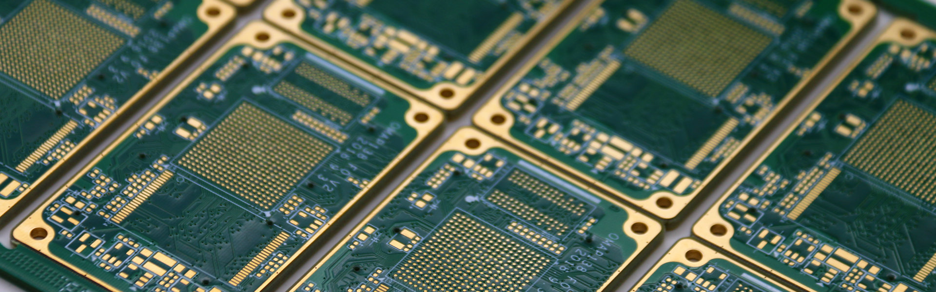
Jinghon Electronics Limited is a professional rigid circuit board (PCB) and flexible printed circuit board (FPC) production enterprises, the products used in TELECOMMUNICATIONS, AUTOMOTIVE ELECTRONICS, 3G PRODUCTS, RF, NETWORKING, SECURITY, INDUSTRIAL CONTROL, MEDICAL, INSTRUMENTATION INSTRUMENTATION, MILITARY PRODUCTS, COMPUTER PERIPHERALS AND OTHER HIGH-TECH FIELDS.
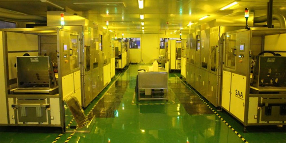
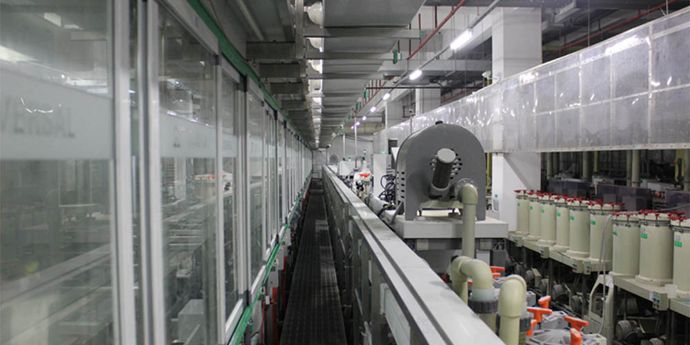
With a facility area of more than 10,000 square meters,Jinghon Electronics Limited is able to produce over 160,000 square meters per year and more than 13,000 items per month, whose PCB products range from 1 to 32 layers, Rigid-Flex, Heavy Copper, HDI, and Embedded Capacitance, and provides "PCB One-stop Shop" service to meet customers’ diverse demands.
CAPABILITY
| Item | Manufacturing Capabilities | Remark | ||||||
|---|---|---|---|---|---|---|---|---|
| MATERIAL | ||||||||
| Material | Shengyi FR-4 | Normal TG, Medium TG and High TG | ||||||
| HF | Medium TG and High TG | |||||||
| Ceramic filled High Frequency Board | Rogers 4003/4350, Arlon 25N/25FR | |||||||
| PTFE High Frequency Board | Rogers series, Arlon series, Taconic series | |||||||
| SPECIFICATION | ||||||||
| Surface Finish | HASL with Lead/HASL LEAD FREE | Tin Thickness | 2-40um | |||||
| Board Thickness | 0.6mm≤H≤3.0mm | |||||||
| Immersion Gold (ENIG) | Max. Gold Thickness | 8u" | ||||||
| OSP | Film Thickness | 0.2-0.5um | ||||||
| Hard Gold | Max. Gold Thickness | 2.0um | ||||||
| Immersion Tin | Tin Thickness | 0.8-1.2um | ||||||
| Immersion Silver | Silver Thickness | 0.15-0.25um | ||||||
| Layers | 4 - 40 layers | FR4 Max. 40 layers | ||||||
| Finished Board Thickness | 0.2-6.8 mm | Min. Thickness: 0.2mm (Double-Sided) | ||||||
| Thickness Tolerance | T≥1.0mm | ±10% (Standard PCB) | ±8% (Advanced PCB) | / | ||||
| T<1.0mm | ±0.1mm (Standard PCB) | ±10% (Advanced PCB) | / | |||||
| Finished Copper Thickness | 1oz/2oz (Standard PCB) | Inner Layer: 12oz (Advanced PCB) | 1oz = 35um | |||||
| Outer Layer: 15oz (Advanced PCB) | ||||||||
| Bow and Twist | Per Cater-Corner Length, ≤0.75% (Standard PCB) | ≤0.50% (Advanced PCB) | For Boards without SMT, the max. 1.5% | |||||
| DRILL | ||||||||
| PTH Deviation | ±3mil (Standard PCB) | ±2mil (Advanced PCB) | ||||||
| NPTH Deviation | ±2mil (Standard PCB) | ±1mil (Advanced PCB) | ||||||
| Hole Position Deviation | ±3mil (Standard PCB) | / | ||||||
| Hole Wall Roughness (Max.) | 1.5mil (Standard PCB) | 1mil (Advanced PCB) | ||||||
| Min. Drilling Bit Diameter | 0.3mm (Standard PCB) | 0.25mm (Advanced PCB) | ||||||
| Max. Drilling Bit Diameter | 6.5mm (Standard PCB) | / | For vias larger than 6.5mm, multiple drilling or milling is recommended | |||||
| Min. Slot Width | 0.6mm (Standard PCB) | / | For HASL, the min. finished slot width is 0.45mm, for other surface finish, it is 0.5mm | |||||
| Board Thickness/Via Diameter | ≤6:1 (Standard PCB) | ≤7:1 (Advanced PCB) | 7:1≤value≥6:1, add one more day for fabrication | |||||
| PTH Deviation | Width | ±4mil (Standard PCB) | / | |||||
| Length | ±5mil (Standard PCB) | / | ||||||
| NPTH Deviation | Width | ±3mil (Standard PCB) | / | |||||
| Length | ±4mil (Standard PCB) | / | ||||||
| Hole Wall Copper Thickness | Thinnest | ≥0.71mil (Standard PCB) | ≥1mil (Advanced PCB) | |||||
| Average | ≥0.8mil (Standard PCB) | ≥1mil (Advanced PCB) | ||||||
| VIA Space (Same Net) | ≥8mil (Standard PCB) | ≥6mil (Advanced PCB) | ||||||
| VIA Space (Different Net) | ≥17mil (Standard PCB) | ≥14mil (Advanced PCB) | ||||||
| Min. Space for Component VIAs in Different Net | ≥24mil (Standard PCB) | ≥20mil (Advanced PCB) | ||||||
| Max. PTH | Round Hole | 8mm (Standard PCB) | 10mm (Advanced PCB) | |||||
| Slot Holes | 6*10mm (Standard PCB) | 8*12mm (Advanced PCB) | ||||||
| TRACE | ||||||||
| Min. Trace Width/Space | 1oz | 6/6mil (Standard PCB) | 5/5mil (Advanced PCB) | The space refers to the distance between trace to trace, trace to copper | ||||
| 2oz | 8/8mil (Standard PCB) | 7/7mil (Advanced PCB) | ||||||
| Min. SMD Width | 1oz | ≥10mil (Standard PCB) | ≥8mil (Advanced PCB) | / | ||||
| 2oz | ≥12mil (Standard PCB) | ≥10mil (Advanced PCB) | ||||||
| Space between Pad to Trace | 1oz | 8mil (Standard PCB) | 6mil (Advanced PCB) | / | ||||
| 2oz | 8mil (Standard PCB) | 6mil (Advanced PCB) | ||||||
| Min. Etching Letters | ≥8mil (Standard PCB) | ≥7mil (Advanced PCB) | ||||||
| Min. Space for SMD | ≥10mil (Standard PCB) | / | The data is the Min. space to achieve Solder Mask Bridge, if Bridge is not required, please refer to the Min. Trace Space requirement | |||||
| V-Cut Line to Copper | T≥1.5mm, V-Cut 20° | 20mil (Standard PCB) | 16mil (Advanced PCB) | |||||
| T≤1.2mm, V-Cut 20° | 16mil (Standard PCB) | 12mil (Advanced PCB) | ||||||
| Trace Width/Space Deviation | ±20% (Standard PCB) | ±15% (Advanced PCB) | ||||||
| Trace Net Grids | 12/12mil (Standard PCB) | 8/8mil (Advanced PCB) | ||||||
| Alignment Accuracy for Layer | ±3mil (Standard PCB) | ±2mil (Advanced PCB) | ||||||
| Space between Trace and Border | Inner layer | ≥16mil (Standard PCB) | ≥12mil (Advanced PCB) | If there is V-Cut requirement, please follow the V-Cut standards | ||||
| Outer layer | ≥10mil (Standard PCB) | ≥8mil (Advanced PCB) | ||||||
| Space between Via to Trace | ≥12mil (Standard PCB) | ≥10mil (Advanced PCB) | ||||||
| Space between Inner Via to Trace | ≥10mil (Standard PCB) | ≥8mil (Advanced PCB) | ||||||
| SOLDER MASK | ||||||||
| Solder Oil Thickness | Trace Interface | 0.4-0.8mil (Standard PCB) | / | |||||
| Trace Corner | ≥0.2mil (Standard PCB) | / | ||||||
| Plugged Via Diameter | Plugged on both sides | ≤0.45mm (Standard PCB) | 0.5-0.55mm (Advanced PCB) | No solder mask opening on both sides | ||||
| Plumpness for Plugged Vias(Max.) | 100%(Vias Diameter≤0.4mm) (Standard PCB) | 50%(Vias Diameter≤0.45mm) (Advanced PCB) | Refer to plugged depth | |||||
| Space between Opening to Trace/Copper | ≥4mil (Standard PCB) | ≥3mil (Advanced PCB) | ||||||
| Opening Size (Single Side) | ≥3mil (Standard PCB) | ≥2mil (Advanced PCB) | ||||||
| Text Width for Solder Mask Opening | ≥10mil (Standard PCB) | ≥8mil (Advanced PCB) | ||||||
| Solder Mask Bridge Width | Green, Blue≥4mil; White, Black≥6mil; others≥5mil | |||||||
| SILKSCREEN | ||||||||
| Silkscreen Width | Positive Text | ≥6mil (Standard PCB) | 5mil (Advanced PCB) | |||||
| Negative Text | ≥8mil (Standard PCB) | ≥6mil (Advanced PCB) | ||||||
| Silkscreen Height | ≥40mil (Standard PCB) | ≥30mil (Advanced PCB) | ||||||
| Space between Silkscreen to Copper Pad | ≥7mil (Standard PCB) | 6mil (Advanced PCB) | ||||||
| The Distance between Solder Mask Oil to Copper Pad | ≥10mil (Standard PCB) | 8mil (Advanced PCB) | The Min. Solder Mask Oil Strip is 5mil | |||||
| Space between Silkscreen to Border | ≥8mil (Standard PCB) | 6mil (Advanced PCB) | ||||||
| Min. Silkscreen Space | ≥6mil (Standard PCB) | 5mil (Advanced PCB) | ||||||
| V-CUT | ||||||||
| Min. Dimension | 80*80mm (Standard PCB) | / | Only for V-Cut with one direction, the min. size is 40mm for the side without V-Cut | |||||
| Max. Dimension | 500*500mm (Standard PCB) | Max. Width for manual V-Cut board is 500mm, not limited for length | ||||||
| Min. Board Thickness | 0.6mm (Standard PCB) | / | No V-cut for 0.4mm board | |||||
| V-CUT Angle | 20°/30° (Standard PCB) | / | ||||||
| Alignment Accuracy for Neighbouring V-CUT | ±0.1mm (Standard PCB) | / | ||||||
| Space for two V-CUT Lines | ≥3mm (Standard PCB) | / | ||||||
| Space between Border to first V-Cut Line | ≥3mm (Standard PCB) | / | ||||||
| Remaining Board Thickness after V-Cut | 1/3 or 1/4 of Board Thickness (Standard PCB) | / | Min. remaining thickness 0.25mm | |||||
| Remaining Board Thickness Deviation after V-Cut | ±0.1mm (Standard PCB) | / | ||||||
| PROFILING | ||||||||
| CNC Routing Deviation | ±0.15mm (Standard PCB) | ±0.10mm (Advanced PCB) | ||||||
| CNC the Distance Deviation between Via to Border | ±0.13mm (Standard PCB) | ±0.10mm (Advanced PCB) | ||||||
| Min. Slot Width | 0.8mm (Standard PCB) | / | ||||||
| CNC Min. Via Corner Angle for Routing | 0.4mm (Standard PCB) | / | ||||||
| Min. PCB Dimension | 5*5mm (Standard PCB) | Min. 3mm for one side (Advanced PCB) | ||||||